History of Nvidia Gaming GPUs: From NV1 Chips to RTX 5090
These days, gaming visuals are nearly unrecognizable compared to the 90s—with ray tracing, DLSS, and a whole arsenal of cutting-edge tech (ambient occlusion, anti-aliasing, different kinds of texture filtering, and more), we’re truly living in the golden age of 3D computer graphics. But it wasn’t always like this.
Over thirty years, Nvidia has grown from a little-known startup into a manufacturer that sets standards in both gaming and data centers. To understand why each new generation of graphics processing units (GPUs) creates such resonance, it is important to trace the chain of decisions and compromises made since 1993.
Let’s take a look at the evolution of Nvidia GPUs for gaming and how the crypto mining boom, followed by the rise of AI-driven technologies, shaped the company’s path (sometimes at the expense of gamers who just wanted to play).
Why Do We Need an Nvidia GPU History?
- The technological context. The GPU market has been evolving at an explosive pace: from fixed-function 3D to general-purpose parallel computing.
- Business lessons. Positioning its chips against 3dfx, ATI, and Intel shows how critical it is to combine innovation with proper time to market.
- Cultural influence. Nvidia shaped esports standards, indirectly influenced filmmaking, and later propelled the wave of generative AI.
We group products by architecture and lithography node, rather than by release year, to reflect logical leaps: from RIVA to GeForce, then Tesla, etc.
Nvidia Origins, NV1 (1993-1995)
Three enthusiastic engineers—Jensen Huang (ex-LSI Logic), Chris Malachowsky, and Curtis Priem (both from Sun)—founded Nvidia on April 5, 1993, in San Jose. Their ambition was a simple system on a chip capable of accelerating both 2D GUIs and 3D games.
First chip—NV1
The NV1 chip (1995) combined graphics, sound, and even a port for the Sega controller. Using quadratic curves instead of polygons created incompatibility with the nascent Direct3D, and a shortage of games quickly buried the project. Nevertheless, the NV1 provided the team with invaluable experience working with integrated multimedia units and the PCI interface.

Era of Nvidia RIVA (1997-1999)
The failure of NV1 forced Nvidia to switch to a fully DirectX-compatible renderer and focus on pure speed.
First success—RIVA 128
The RIVA 128 (1997) offered 3.3 million transistors on a 350 nm process, full-fledged 3D in 32-bit color, and a bandwidth of 1.6 GB/s at a price lower than Voodoo Graphics (but with inferior texture filtering). Massive OEM contracts with Dell and Gateway helped to make Nvidia profitable in just one quarter.
Nvidia vs ATI and 3dfx—TNT and TNT2
In 1998, Twin-Texel (TNT) doubled the pipelines and introduced a 32-bit Z-buffer, but it was losing to Voodoo2 (3dfx) in clock speed. The revised TNT2 (1999), running at 250 MHz, beat the competition (Rage 128 series from ATI) and laid the foundation for the GeForce brand. Nvidia proved that it could release annual DirectX-compatible updates, keeping up with price and performance.
GeForce: The First Nvidia GPU (1999-2003)
The GeForce 256 (NV10) was released in the fall of 1999 and, for the first time, integrated a fixed-function T&L (transform, clipping, and lighting) pipeline directly on the chip, delivering up to 15 million triangles/s at 120 MHz. The marketing term GPU emphasized the difference from competitors’ 2D/3D accelerators and disrupted 3dfx’s roadmap—now it had to catch up in hardware transformations.

GeForce 2 GTS/Ultra (2000) doubled the texture units and moved to a 180 nm process, offering a fully multithreaded detonator driver for the first time. GeForce 3 (NV20, 2001) added programmable vertex and pixel shaders (DX8) and introduced nfiniteFX technology, allowing developers to implement bump mapping and per-pixel lighting effects in shaders rather than via fixed tables.

The improved GeForce 4 Ti (2002) removed the memory bottleneck through the LMA II cache and introduced Accuview AA, maintaining the lead over ATI Radeon 9700. In parallel, the GeForce 4 MX line offered a stripped-down DX7 feature set for laptops, effectively marking Nvidia’s expansion into the mobile segment. Fifth generation (2003) introduced programmable shader functionality.

Nvidia Curie and Tesla: GPU Architecture Cycle Begins (2004-2008)
In 2004, with GeForce 6 (NV40), there was a clear two-year architecture cycle plus a half-year interval for rebranding. The main features were SLI (two PCIe cards linked by a bridge) and Shader Model 3.0 with dynamic branches. The transition to GeForce 7 (G70, 2005) on 90 nm increased density to 302 million transistors and introduced Transparency AA, while the revision of G71 delivered the first single-chip card that surpassed the previous generation’s dual-SLI setup.

The Tesla architecture (G80, 2006) was a leap forward: unified ALUs, 128 stream processors, and CUDA 1.0 support. The GeForce 8800 GTX not only accelerated games with HDR and DX10, but also opened the way for GPGPU: early Folding@home projects showed a ten-fold speed-up over CPUs, setting the stage for future data-center A100s.
Fermi to Kepler: Nvidia’s Efficiency Breakthrough (2009-2013)
Fermi (GF100, GeForce 400/500) added L1/L2 caches, ECC, and per-core dynamic clocking, but the initial 40 nm chip was notorious for its heat output—250 W TDP for the GTX 480.
A breakthrough in energy efficiency came with Kepler (GK104, 2012): 28 nm, the removal of heavy double-precision units from consumer GPUs, and the introduction of GPU Boost 1.0, which automatically raises clock speed as long as it remains within the thermal budget. The GeForce GTX 680 became the benchmark for watts per frame, and the server-oriented GK110 brought back FP64 support for Tesla K20X cards and Cray Titan–class supercomputers.
Nvidia Maxwell (2014-2015)
Maximizing density, Maxwell (GM204/GM200) redesigned the SM cluster, reducing power consumption to 165 W while raising FPS by a third compared to Kepler. The GeForce GTX 980/970 on 28 nm showed that energy efficiency is more important than raw power, and support for HDMI 2.0 and asynchronous timewarp made the cards VR-Ready.
Maxwell laid the foundation for a future transition to deep block optimization for a better FPS-per-watt ratio.
Nvidia Pascal: AI Acceleration (2016-2017)
With the release of Pascal, Nvidia transformed the GPU from a graphics accelerator into a universal AI engine. TSMC’s 16 nm process allowed the GP104 (GeForce GTX 1080) to pack 3,584 CUDA cores and deliver 11 TFLOPS of FP32 performance, boosting energy efficiency by around 70% compared to Maxwell.
For the first time, the flagship GP102-based Titan X/Xp included hardware support for FP16 (doubling operation density), bridging to future neural-network workloads. The NVLink 1.0 bus connected multiple Pascal cards at up to 80 GB/s, eliminating the PCIe bottleneck in HPC clusters. In 2016, the DGX-1 server showed that eight Tesla P100s could train Inception-v3 faster than dozens of CPU nodes in a single day; this is how the AI-appliance market was born.
Nvidia Turing: Real-Time Ray Tracing (2018-2019)
The Turing architecture (TU102/104) brought two new compute units: RT cores for hardware BVH traversal and second-generation tensor cores for matrix operations. In games, this materialized as the GeForce RTX 20-series (2018) and DLSS 1/2, which performs supersampling via a trained neural network.
RTX 2080 Ti became the first card capable of real-time ray tracing at 60 fps. The Quadro RTX professional line delivered the same capabilities to CAD and DCC workloads, allowing designers to render final-quality global illumination directly in the viewport with almost no need for prerenders.
Nvidia Ampere: More Power and AI (2020-2022)
The pandemic years did not slow Nvidia down: while interest in PC games was at an all-time high, Ampere moved to Samsung’s 8 nm node and launched the RTX 30 family, doubling tensor and RT-core throughput. PCIe 4.0 unlocked the potential of Resizable BAR and fast SSDs for texture streaming.
However, the surge in cryptocurrency mining caused severe shortages, prompting the release of Lite Hash Rate (LHR) variants to curb Ethereum mining demand. In data-center A100 parts (GA100, 7 nm), TSMC’s process enabled 312 TFLOPS of FP16 performance and structured sparsity, cementing Ampere as the standard for training GPT-3-class models.
Nvidia’s inability (or some would argue it was perceived reluctance) to fix the problem angered regular gamers. But the problem solved itself when Ethereum transitioned to Proof-of-Stake, effectively ending GPU-based mining.
Nvidia Ada Lovelace: DLSS 3 and Frame Generation (2022-2023)
TSMC’s 4N process and a record-breaking 76.3 billion transistors raised the bar with Ada Lovelace. The GeForce RTX 40 series received DLSS 3 with Frame Generation: optical-flow inference inserts synthetic frames, doubling FPS without increasing shader load. The RTX 4090 delivers up to 100 TFLOPS of FP32 while staying within a 450 W TDP, thanks to fourth-generation GPU Boost.
The RTX Laptop GPU Gen 5 line brings the same AD103/106 core with Dynamic Boost 2.0 and Advanced Optimus, making slim 16 mm designs viable for Blender Cycles and Unreal Engine 5 Lumen.
The architecture shows that synergy among RT, tensor, and classic ALU blocks is becoming key not only to Nvidia’s visual evolution but also to its computational progress. Due to the AI boom, Nvidia began earning more from data center GPUs than from gaming cards.

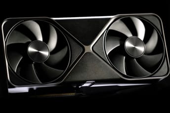
Nvidia Blackwell: RTX 50-series (2024-present)
The Blackwell architecture (B100/B200) moved to a redesigned TSMC 5 nm chiplet layout and introduced DLSS 4 with Multi-Frame Generation: the algorithm inserts a few AI frames per render frame, multiplying FPS. This architecture ushers in the GDDR7 era: a 512-bit bus and speeds up to 28 Gbps provide 1.8 TB/s, eliminating the main bottleneck of the RTX 40-series.
The flagship GeForce RTX 5090 carries 92 billion transistors, 32 GB of VRAM, and more than 3 PFLOPS of tensor performance, delivering roughly double the 4K frame rate of the RTX 4090. The mainstream RTX 5070/5060 reduces the number of GPC clusters but retains 4th-generation RT cores and full DLSS 4 support, potentially covering the mid-budget segment (if we forget about the scalping problem).
Nvidia now earns several times more from data centers (which significantly influencing it) than from gaming, making them the company’s main revenue stream. This shift is reflected in the RTX 50-series launch: various technical issues, a baffling 8GB RTX 5060 Ti, and the inability to buy cards at MSRP—all while AMD Radeon and even Intel Arc are catching up.
Nvidia GPU Generations
- Celsius, 1999 (GeForce 256 and GeForce 2 series)
- Kelvin, 2001 (GeForce 3 series and GeForce 4 series)
- Rankine, 2003 (GeForce 5 series)
- Curie, 2004 (GeForce 6 series and GeForce 7 series)
- Tesla, 2006 (GeForce 8 series, GeForce 9 series, GeForce 100 series, GeForce 200 series, and GeForce 300 series)
- Fermi, 2010 (GeForce 400 series and GeForce 500 series)
- Kepler, 2012 (GeForce 600 series, GeForce 700 series, and GeForce 800M series)
- Maxwell, 2014 (GeForce 700 series, GeForce 800M series, GeForce 900 series)
- Pascal, 2016 (GeForce 10 series, Quadro P, and Tesla P4)
- Turing, 2018 (GeForce 16 series and GeForce 20 series)
- Ampere, 2020 (GeForce 30 series)
- Ada Lovelace, 2022 (GeForce 40 series)
- Blackwell, 2025 (GeForce 50 Series)
FAQ
What does the “128” in Nvidia RIVA 128 mean?
It refers to the 128-bit memory interface.
What was the first RTX graphics card?
Nvidia GeForce RTX 2080 (2018).
What was the first graphics card?
IBM Monochrome Display Adapter (MDA), 1981.
When was Nvidia founded?
Nvidia was founded on April 5, 1993.
When did the 20 series come out?
In September 2018.
Where are Nvidia graphics cards made?
Nvidia designs chips in the U.S., but they’re manufactured by TSMC (Taiwan) and Samsung (South Korea).
Summary of Nvidia History
Over the past 30 years, the company has come a long way—from a small startup to a global leader in graphics and AI computing. At GTC 2025, Jensen Huang announced the Blackwell Ultra (B300): 288 GB of HBM4 and up to 20 PFLOPS FP8 in a single-die assembly.
Further down the roadmap are the Vera Rubin (2026) and Feynman (2028) families with NVL576 configurations—chiplet arrays with optical interposers, UCIe interfaces, and specialized Inference Tiles separated from graphics blocks.
All of this sounds impressive, but the question remains whether gaming will still be a priority—or just a legacy market in a broader technological race. Nvidia may be shaping the future of computing, but for many gamers, even buying a GPU today feels like a battle—one they’re no longer sure they’re meant to win.