GPU Without Factories: Inside Nvidia’s Fabless Business Model
|
|
Nvidia is one of the most recognizable names in gaming and simultaneously the market leader in AI accelerators—yet it does not own a single lithographic facility. Despite this, millions of graphics cards are sold each year, while data centers are packed with Hopper accelerators, whose postage stamp-sized dies are engineered to handle hundreds of watts of thermal load.
So, where does the hardware come from if Nvidia’s physical presence in California consists mostly of offices and R&D labs? The answer lies in its fabless business model. Nvidia focuses on chip design and its software ecosystem, outsourcing all heavy industrial processes to specialized external contractors. As a result, every RTX GPU is the outcome of a global collaboration: chip architecture from Santa Clara, lithography in Taiwan, advanced packaging in South Korea, and final assembly in various facilities across the world (mostly China).
By tracing this chain step by step, we can better understand why manufacturer’s suggested retail price (MSRP) often fails to align with real pricing, what influences some rare units sought after by collectors and overclockers, and how global disruptions are almost immediately reflected on local store shelves.
Nvidia GPU Development: From Design to Verification
Architecture and IP cores
Inside every GPU lies a complex system of modular components known as semiconductor intellectual property cores (or simply, IP cores): Streaming Multiprocessors (SMs), RT cores for real-time ray tracing, tensor cores for AI tasks, video encoders/decoders, memory controllers, and PCIe interfaces.
The architectural team in Santa Clara determines the composition of these blocks for each new generation: how many are needed, what new instructions will be added to the instruction set architecture (ISA), and how to balance performance, die area, and power efficiency.
RTL design and simulation
Once the high-level architecture is finalized, engineering centers in Israel, India, and China take over the register-transfer level (RTL) design. At this stage, millions of lines of code are written and fed into industrial-grade simulation tools. The designs undergo formal verification, fuzz testing, and stress benchmarks that simulate both AAA-gaming scenes and workloads from large language models (LLMs).
Physical implementation and place & route
After the logic design is complete, physical implementation begins. The place and route (P&R) stage involves arranging standard cells, routing copper and cobalt interconnects, and embedding static random-access memory (SRAM) blocks. Engineers perform meticulous checks for electromigration, thermal hotspots, and signal integrity. Multiple P&R iterations may take months to meet the strict power, efficiency, and size targets.
Tape-out and risk wafer
The completed GDSII file (the digital blueprint of the chip) is then sent for initial fabrication (which is called tape-out) as a risk wafer (test dies produced to validate the wafer’s design in practice). If the result meets specifications in terms of performance and defect density, it paves the way for mass production. If not, the design is sent back for revision.
This is why thorough verification carries more weight than any marketing deadline: a faulty chip caught late in the pipeline can result in months of delay and millions in additional cost.
Made in Taiwan
Nvidia’s role is not building factories, but transferring blueprints to the global leader in semiconductor contract manufacturing, Taiwan Semiconductor Manufacturing Company (TSMC). It is on TSMC’s advanced production lines that the majority of modern chips for GPUs are fabricated (from Ampere and Ada Lovelace to Blackwell architecture). Each wafer undergoes hundreds of photolithographic, diffusion, and metallization steps before being transformed into dozens of gleaming silicon dies.
Processing cost
Some nodes rely on deep ultraviolet (DUV) lithography with multiple patterning stages, while the shift to next-gen technologies introduces extreme ultraviolet (EUV) masks. EUV reduces the number of processing steps but requires ultra-precise and expensive ASML scanners. As a result, a single 300 mm wafer used for top-end chips like the RTX 5090 can exceed $20,000 in cost. The final price of a usable die reflects the complexity of dozens of metal layers, as well as the extensive yield and performance testing involved.
Why outsource to TSMC instead of building an Nvidia factory
Building a state-of-the-art 3nm fab costs billions of dollars and requires years to recoup. Nvidia’s fabless strategy allows it to allocate those resources to software development (such as CUDA, drivers, and AI frameworks) while shifting manufacturing risks to its partners. It also provides strategic agility: during each node transition, Nvidia simply secures new allocation slots without the burden of physical infrastructure.
Alternatives and contingency strategies
In 2020, due to a global capacity crunch, Nvidia temporarily turned to Samsung’s 8nm process for Ampere GPUs. However, the resulting chips suffered from reduced overclocking headroom and higher power consumption. As soon as capacity allowed, Nvidia reverted to TSMC.
Today, advanced components like chip-on-wafer-on-substrate (CoWoS) and HBM interposers for H100 and H200 data center accelerators are also sourced from TSMC, with production queues reserved 12+ months in advance.
Wafer sorting
After lithographic processing, wafers are diced, and each individual die undergoes electrical testing. Engineers measure maximum stable frequencies at various voltages and identify defects in through-silicon vias (TSVs). The higher the yield of high-quality chips, the more GPUs reach add-in board (AIB) partners, improving prospects for end-user overclocking and boosting performance consistency in the retail market.
OSAT and Chip Packaging
When the dies leave TSMC, they are handed to outsourced semiconductor assembly and testing (OSAT) providers for dicing, ball-grid formation, and final inspection before high-volume assembly. Industry leaders (ASE Technology, Amkor, JCET, and StatsChipPAC) receive the wafers, laser-cut them into individual dies, form dense micro-bump arrays, inject underfill to reinforce the joints, and solder each chip onto a multilayer organic substrate.
For flagship accelerators, the workflow is even more complex. TSMC performs CoWoS packaging, integrating the GPU die, HBM3 stacks, and a retimer chip on a shared silicon interposer.
Once sealed, the module undergoes burn-in (usually at 125 °C) under elevated clocks to expose latent metallization flaws. Only dies that pass this screening earn known-good die (KGD) status and receive serial numbers that later indicate stepping and overclocking headroom. Packaging defects at this stage can scrap up to 10% of a wafer, so OSAT precision directly influences the eventual cost of every GPU.
From PCB to Finished GPU: The Role of Add-in-Board Partners
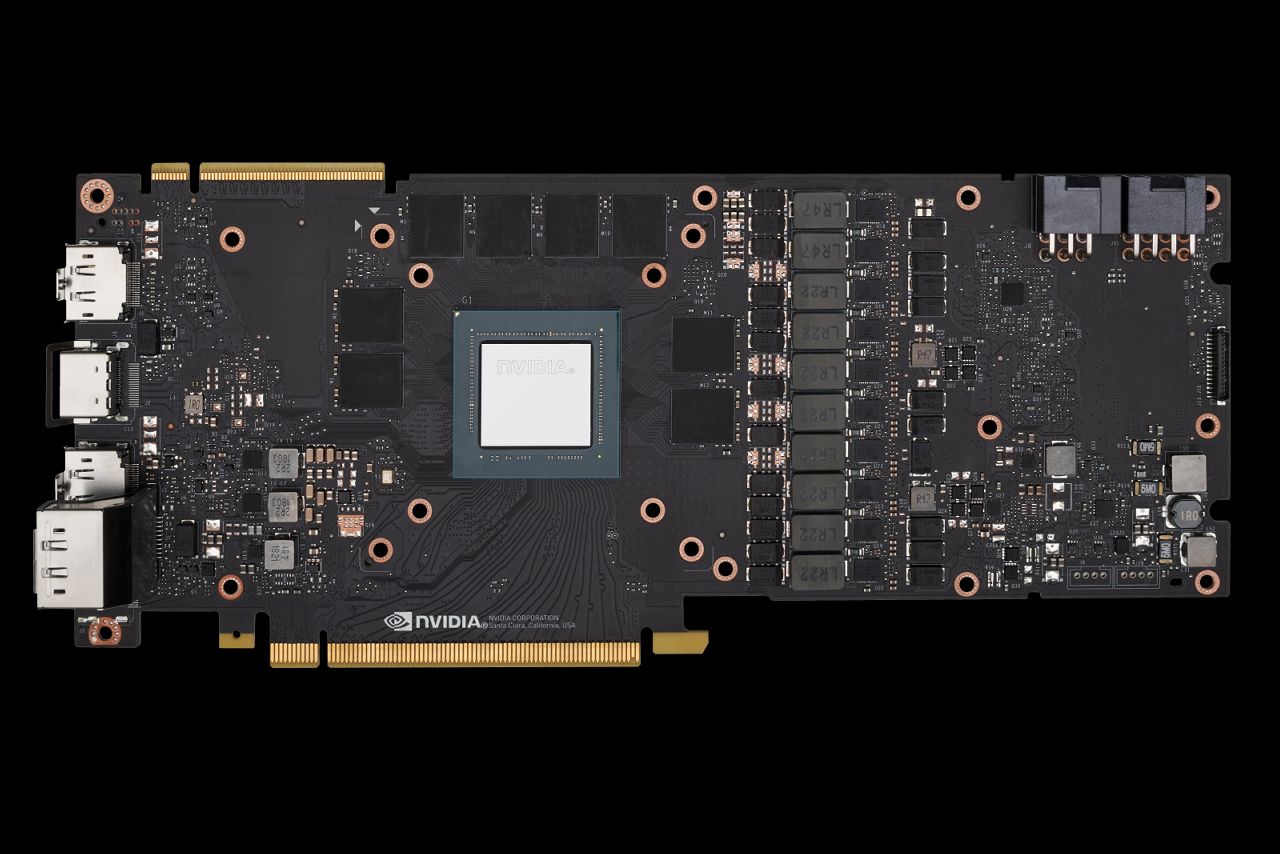
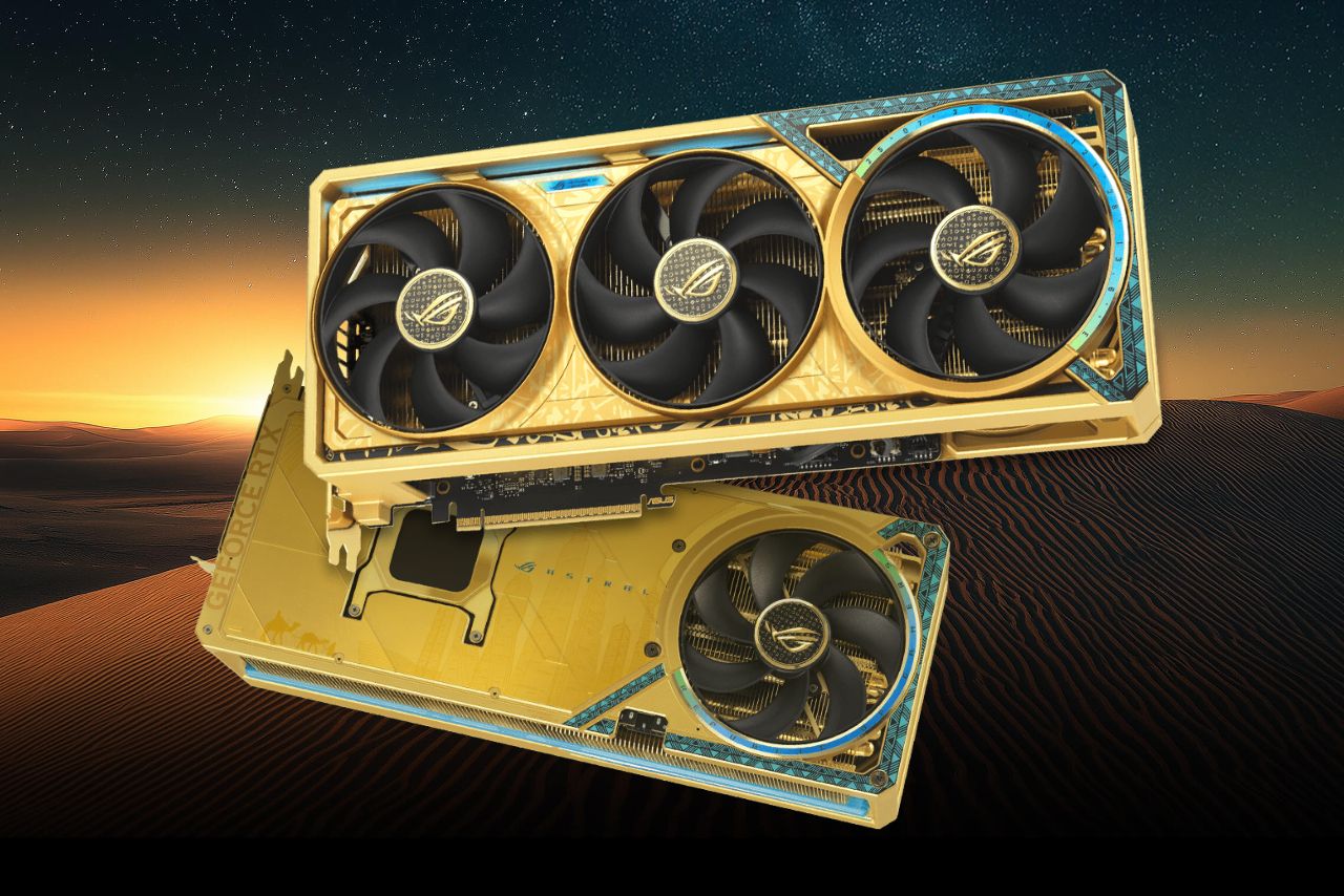
The next phase belongs to AIB partners: companies like ASUS, MSI, Gigabyte, Palit/Gainward, Zotac, Colorful, Inno3D, as well as niche vendors like PNY and Sparkle. These manufacturers purchase bare chips or pre-mounted test assemblies and build complete retail graphics cards around them. The process begins with a custom printed circuit board (PCB) design.
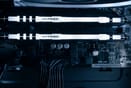
- Power delivery. Engineers develop VRM systems with 14 to 26 power phases, selecting appropriate DrMOS modules, chokes, and low-ESR capacitors capable of handling hundreds of watts of peak load from flagship GPUs
- PCB layout. Multi-layer boards are used to isolate power delivery from high-speed RAM traces, reducing signal interference and electromagnetic crosstalk.
- Firmware. BIOS programming defines power limits, fan curves, and factory overclocking presets, resulting in different stock keeping units (SKUs) like “OC”, “Gaming X”, etc.
In parallel, thermal design teams engineer cooling systems: nickel-plated copper bases, vapor chambers, heat pipes, and dense aluminum fin stacks. 90-120 mm fans with dual ball bearings provide airflow, while aesthetic touches like RGB lighting and custom backplates distinguish each brand. Proprietary cooling innovations include ASUS’s Axial-tech and more.
AIB final touches
Production is typically located in Shenzhen, Suzhou, or Da Nang. However, leading brands also operate facilities in Europe: MSI runs an assembly plant in Ostrava for the EU market, while Gigabyte produces some Gaming OC models in the Czech Republic. After automated optical inspection (AOI), completed cards are shipped to regional distributors and then to retailers and system integrators.
The fierce competition among AIBs results in hundreds of variations of the same Nvidia GPU: quiet, oversized triple-fan models, compact ITX designs, or custom-loop water-cooled editions. However, this diversity also leads to market fragmentation.
Premium components (additional power phases or advanced coolers, for example) inflate costs, and top-binned dies with the highest frequency tolerance are reserved for flagship variants. Consequently, the gap between MSRP and real prices often widens, as seen during mining booms or recent spikes in AI demand.
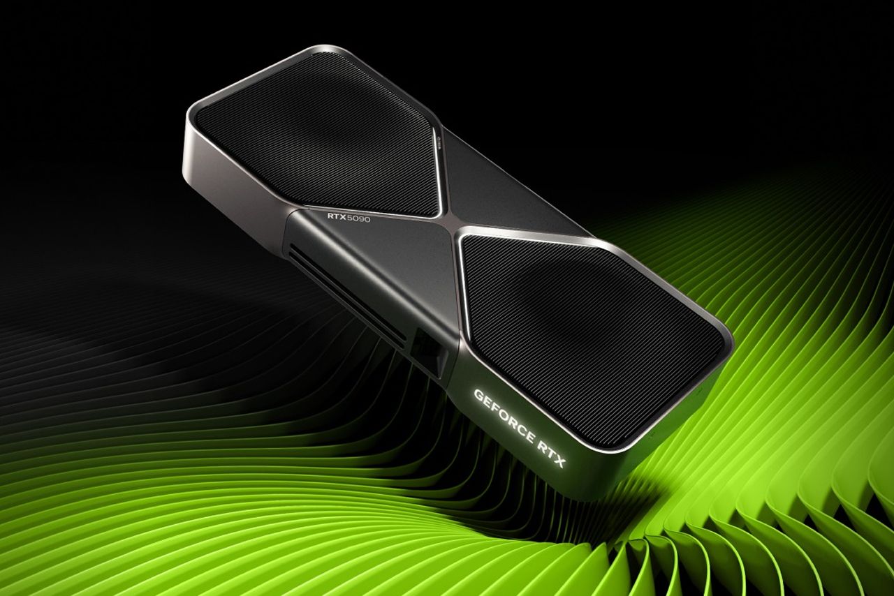
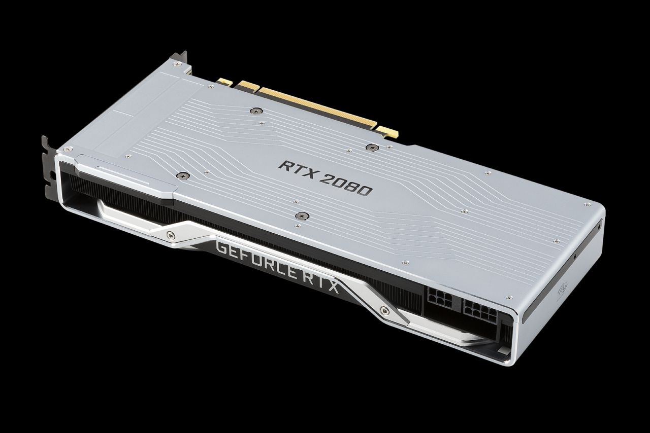
Founders Edition GPU: Nvidia’s Own Benchmark for the Market
To establish the visual and engineering baseline for each new generation of graphics cards, Nvidia has offered its own Founders Edition (FE) models since the Pascal architecture. These are not produced in-house, but are assembled under contract by manufacturers (usually Foxconn or BYD), often on the same lines used for iPhones or Dell laptops.
Nvidia handles the design of both the PCB and the cooling system: an aluminum monoblock with a vapor chamber for the GTX 1080, a dual-axis heatsink for the RTX 30 series, and a flow-through end-to-end design for the RTX 50 series.
Founders Edition GPUs serve three core purposes
- Benchmark. AIB partners receive a functional reference design, which helps in analyzing thermal behavior and component layout
- Marketing. Review units sent to the media are based on identical hardware, enabling consistent, generation-over-generation comparisons
- MSRP control. By selling FE cards at the suggested retail price through NVIDIA’s webstore and select partners, the company attempts to limit artificial scarcity and speculative markup
FE model availability is typically limited, and sales are synchronized with the global embargo lift. As a result, they tend to sell out instantly, often scooped up by scalpers or enthusiasts who value the compact PCB layout and minimalistic design, free from flashy RGB lighting or other design choices without actual benefits in performance. Additionally, Nvidia Founders Edition graphics cards have a dedicated driver configuration entry, allowing custom fan curves and power limits (features that simplify manual overclocking and general use for enthusiasts).
Proof of concept
The Founders Edition allows Nvidia to demonstrate how far a GPU can be pushed in terms of performance, thermals, acoustics, and aesthetics without third-party embellishments, after which AIB partners take over, offering countless variants built on the same silicon foundation.
Logistics: How a Nvidia GPU Becomes a Product on the Shelf
After OSAT processing and AIB assembly, finished graphics cards are packed into master cartons (typically 10-20 units per box) and shipped from via two main routes.
- Sea freight (60-70% of volume). Containers depart from ports like Shenzhen or Ningbo, transit through hubs (Singapore, the Suez Canal, etc.), and arrive in Rotterdam, Hamburg, or Los Angeles within a month. This method costs just a fraction of a dollar per GPU but involves significant lead time and safety buffering
- Air cargo (usually for flagships and launch waves). Charter flights from Incheon or Shenzhen to Leipzig or Memphis reduce factory-to-warehouse time to under 72 hours, but the cost rises to a few dollars per unit
At the destination, cargo clears customs: in the EU, the import tariff is 0% (HS code 8473 30 20), while in the US situation is very complicated right now (and changes almost every week). From there, cards move to regional distributors (Tech Data, Ingram Micro, Esprinet, and many more), which then break shipments into smaller lots for e-tailers and system builders.
Any disruption (a delayed container, spike in freight rates, or export bottleneck) immediately impacts price and availability. This was a key reason for the RTX 4090 Ti delays: TSMC’s CoWoS capacity and air cargo lanes were saturated with H100 data center shipments.
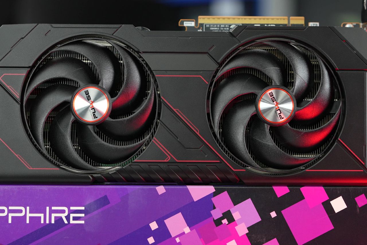
Nvidia vs AMD: Two Different Fabless Models
Like Nvidia, AMD is a fabless company that relies on TSMC and the same OSAT contractors, yet its go-to-market strategy diverges sharply. With every launch, AMD ships sizable batches of made-by-AMD (MBA) reference boards; its GPUs are readily available from day one. This practice anchors street prices and sets a cost/layout benchmark for AIB partners.
- AIB competition level. Fewer GPU dies mean fewer SKUs: the RX 7800 XT had roughly 30 board variants, whereas the RTX 4070 Super—over 60
- BIOS latitude. AMD lets partners adjust voltage and power limits more aggressively, but still keeps some thermal-noise headroom for its own MBAs
- Price volatility. A tighter chip supply makes AMD cards more vulnerable to price spikes (like RX 6800 XT during the 2021 mining boom)
Overall, AMD follows a hybrid approach: it preserves the AIB ecosystem yet reserves a crucial reference niche, using MBA cards to enforce a floor price and coherent market positioning.
Nvidia vs Intel: Fabless Contracting vs Vertical Integration
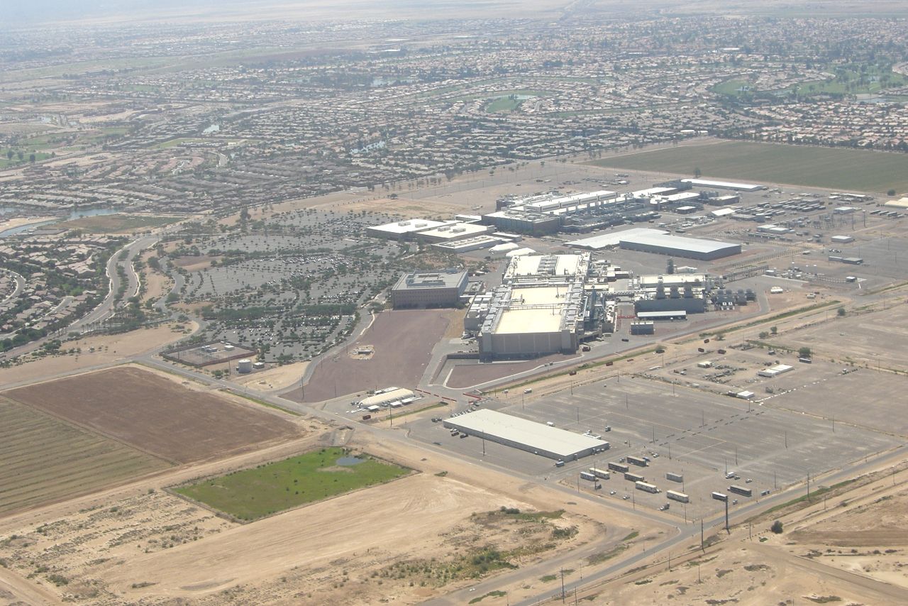
Intel is traditionally an integrated device manufacturer (IDM), designing and producing chips in-house on Intel 7/4 today and 3/18A/20A tomorrow. The Intel Arc GPU line is a rare modern example of a single vendor controlling the entire graphics card pipeline.
- Front-end. Fabs in Arizona and Ireland manufacture DG2 silicon
- Back-end. Assembly and test run in the same facilities that package Xeon CPUs
- Brand mix. Intel ships most Arc boards itself; AIB versions from ASRock or Acer account for less than 20% of volume
Advantages of vertical integration
- Built-in capacity buffers, meaning shorter queues than at TSMC
- End-to-end quality control with unified SPC metrics
- Ability to subsidize MSRP by reallocating margin between fabrications and product units
Drawbacks of vertical integration
- Massive capital expenditure. Each lithography node upgrade costs at minimum over $10 billion
- Limited variety. There are no dozens of AIB options, so fewer niche SKUs
- Internal competition. CPUs and GPUs vie for Intel 4 wafers; in case of shortages, CPUs are priority
Looking ahead, Intel Foundry Services aims to open these fabs to external customers, effectively creating a second TSMC. Should that succeed, Nvidia gains an alternative advanced node, and overall industry dependence on Taiwan diminishes.
How the Supply Chain Shapes GPU Price and Availability
The shelf price of an RTX graphics card is not simply MSRP with added store markup. It is the cumulative result of margins added at every stage of the supply chain.
- Lithography and packaging (~50%). The first (and largest) part of the price is the cost of a wafer. A single 300 mm wafer now runs at least $20,000, driven by EUV scanners and CoWoS interposers. Yield losses during OSAT (assembly, reballing, rework) tack on a further 5-7%
- AIB assembly (~25%). Extra PCB layers, nickel-plated copper bases, vapor chambers, and ultra-quiet fans each add $10-100 to the bill of materials
- Logistics and insurance (~10%). Sea shipment is inexpensive but slow; air freight is fast yet costly. During demand spikes, the air-cargo share rises, and suppliers pay maximum insurance against loss or damage
- Distribution and retail (~15 %). Distributors break bulk lots, warehouse inventory, and extend credit to small resellers. Retailers add marketing, customer service, and return-rate risk, layering on the final markup
What is MSRP?
MSRP stands for manufacturer’s suggested retail price, meaning the price a company recommends retailers charge for a product.
Why MSRP often fails
- Tight margins by design. MSRP assumes each chain accepts minimal profit. Any shock (shortages, copper price volatility, substrate constraints, or new tariffs) breaks that equation overnight
- Scalping. Bots snap up Founders Edition and rare AIB models at launch, shifting scarcity from wholesale to retail
- Currency volatility and taxes. For example, at launch, the RTX 4090 retailed for €1,949 in the EU versus a $1,599 U.S. MSRP. The gap reflects VAT plus a distributor buffer against euro-dollar swings
Conclusion: Single GPU—Dozens of Companies
The GeForce RTX 4070 graphics card inside my PC is the result of a global assembly puzzle. CUDA cores are designed by architects in Santa Clara. TSMC’s lithography lines in Taiwan etched them onto silicon wafers. OSAT facilities in Zhuhai attached HBM stacks and completed the packaging. Engineers at ASUS in Shenzhen built robust triple-fan coolers. The finished product was packed into containers, sailed through the Suez Canal, reached a European distributor, and was finally delivered to a local retailer who added a warranty. Only then did the box with the GPU land on my desk.
This extended chain enables flexibility (hundreds of SKUs, diverse cooling designs, and wide pricing tiers), but also introduces fragility. A wafer shortage, freight spike, or export restriction can instantly lead to empty shelves and inflated prices.
Understanding this process can help you make better-informed decisions: whether to wait for a chance to get the Founders Edition GPU from Nvidia itself, opt for a quiet OC model from an AIB partner, consider an MBA Radeon card, or take a chance on a rising Intel Arc. Behind every logo is a vast network of global contributors, and this invisible to the average consumer ecosystem ultimately decides how much you’ll pay and how soon you’ll get your hands on the latest hardware.